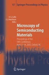
Microscopy of Semiconducting Materials (eBook)
XVI, 540 Seiten
Springer Berlin (Verlag)
978-3-540-31915-3 (ISBN)
The 14th conference in the series focused on the most recent advances in the study of the structural and electronic properties of semiconducting materials by the application of transmission and scanning electron microscopy. The latest developments in the use of other important microcharacterisation techniques were also covered and included the latest work using scanning probe microscopy and also X-ray topography and diffraction.
Epitaxy: Wide Band-Gap Nitrides.- Structural properties of GaN quantum dots.- Stranski-Krastanov growth for InGaN/GaN: wetting layer thickness changes.- Investigation of InxGa1?x N islands with electron microscopy.- First stage of nucleation of GaN on (0001) sapphire.- In GaN-GaN quantum wells: their luminescent and nano-structural properties.- Evolution of InGaN/GaN nanostructures and wetting layers during annealing.- Origins and reduction of threading dislocations in GaN epitaxial layers.- Oxygen segregation to nanopipes in gallium nitride.- Strain relaxation in (Al,Ga)N/GaN heterostructures.- A TEM Study of A1N Interlayer Defects in AlGaN/GaN Heterostructures.- Reduction of threading dislocation density using in-situ SiNx interlayers.- The nucleation structure for cracks in AlGaN epitaxial layers.- Microstructural and optical characterisation of InN layers grown by MOCVD.- Structural properties of InN thin films grown with variable growth conditions on GaN/Al2O3 by plasma-assisted MBE.- Growth and surface characterization of piezoelectric AlN thin films on silicon (100) and (110) substrates.- Characterization and structuring of nitride-based heterostructures for vertical-cavity surface-emitting lasers.- Characterization of defects in ZnS and GaN.- Epitaxy: Silicon-Germanium Alloys.- Use of moire fringe patterns to map relaxation in SiGe on insulator structures fabricated on SIMOX substrates.- TEM measurement of the epitaxial stress of Si/SiGe lamellae prepared by FIB.- Strain relaxation of SiGe/Si heterostructures by helium ion implantation and subsequent annealing: Helium precipitates acting as dislocation sources.- TEM investigation of Si/Ge multilayer structure incorporated into MBE grown Si whiskers.- Local compositional analysis of GeSi/Si nanoclusters by scanning Auger microscopy.- A study of processed and unprocessed dual channel Si/SiGe MOSFET device structures using FIB and TEM.- Epitaxy: Growth and Defect Phenomena.- Novel TEM method for large-area analysis of misfit dislocation networks in semiconductor heterostructures.- Beta to alpha transition and defects on SiC on Si grown by CVD.- Strain relaxation and void reduction in SiC on Si by Ge predeposition.- Defect generation in high In and N content GaInNAs quantum wells: unfaulting of Frank dislocation loops.- Structural characterisation of spintronic GaMnAs and GaMnN heterostructures grown by molecular beam epitaxy.- TEM determination of the local concentrations of substitutional and interstitial Mn and antisite defects in ferromagnetic GaMnAs.- First-principles calculations of 002 structure factors for electron scattering in strained InxGa1?xAs.- Structural characterisation of MBE grown zinc-blende Ga1?xMnxN/GaAs(001) as a function of Ga flux.- Magic matching in semiconductor heterojunctions.- Changes in plasmon peak position in a GaAs/Tn0.2Ga0.8As structure.- Investigation of the electrical activity of dislocations in ZnO epilayers by transmission electron holography.- A TEM study of Mn-doped ZnO layers deposited by RF magnetron sputtering on (0001) sapphire.- High Resolution Microscopy and Nanoanalysis.- Aberration-corrected HREM/STEM for semiconductor research.- Spherical aberration correction and exitplane wave function reconstruction: Synergetic tools for the atomic-scale imaging of structural imperfections in semiconductor materials.- Strain mapping from HRTEM images.- Quantification of the influence of TEM operation parameters on the error of HREM image matching.- ConceptEM: a new method to quantify solute segregation to interfaces or planar defect structures by analytical TEM and applications to inversion domain boundaries in doped zinc oxide.- Electron holography of doped semiconductors: when does it work and is it quantitative?.- Why does a p-doped area show a higher contrast in electron holography than a n-doped area of the same dopant concentration?.- Interference electron microscopy of reverse-biased p-n junctions.- Off-axis electron holography of focused ion beam milled GaAs and Si p-n junctions.- Towards quantitative electron holography of electrostatic potentials in doped semiconductors.- Three-dimensional analysis of the dopant potential of a silicon p-n junction by holographic tomography.- Ab initio computation of the mean inner Coulomb potential for technologically important semiconductors.- Self-Organised and Quantum Domain Structures.- Electron beam induced deposition of position and size controlled structures on the nanometre scale.- The structure of coherent and incoherent InAs/GaAs quantum dots.- Electron microscopy and optical spectroscopy of single InAs/InP quantum dots.- Vertical correlation-anticorrelation transition in InAs/GaAs quantum dot structures grown by molecular beam epitaxy.- Effect of annealing on anticorrelated InGaAs/GaAs quantum dots.- Nanoanalysis of InAs/GaAs quantum dots using low-loss EELS spectra.- Structural analysis of the effects of a combined InAlAs-InGaAs capping layer in 1.3-?m InAs quantum dots.- Microstructural studies of InAs/GaAs self-assembled quantum dots grown by selective area molecular beam epitaxy.- Chemical composition and strain distribution of InAs/GaAs(001) stacked quantum rings.- In distribution in InGaAs quantum wells and quantum islands.- Activation energy for surface diffusion in GaInNAs quantum wells.- Growth and surface structure of silicon nanowires observed in real time in the electron microscope.- Self-catalytic growth of gallium nitride nanoneedles under Garich conditions.- Nanocontacts fabricated by focused ion beam: characterisation and application to nanometre-sized materials.- Cross-sectional studies of epitaxial growth of InP and GaP nanowires on Si and Ge.- Quantitative measurements of the inhomogeneous strain field of stacked self-assembled InAs/InP(001) quantum wires by the Peak Finding Method.- Measurement of the mean inner potential of ZnO nanorods by transmission electron holography.- Quantum effects in band gap-modulated amorphous carbon superlattices.- Structure of rolled-up semiconductor nanotubes.- Defects and interfaces in nanoparticles.- TEM characterization of magnetic Sm- and Co-nanocrystals in SiC.- Microscopy of nanoparticles for semiconductor devices.- Structural and electrophysical properties of a nanocomposite based upon the Si-SiO2 system.- HRTEM and XRD analysis of P6mm and Ia3d double gyroidal WO3 structures.- Processed Silicon and Other Device Materials.- Research highlights and impacts upon industry for nanoelectronics in the university system of Taiwan.- TEM investigations of epitaxial high-? dielectrics on silicon.- Damage layer in silica-based low-k material induced by the patterning plasma process studied by energy-filtered TEM.- Measurement of field-emission properties of a single crystal silicon emitter using scanning electron microscopy.- Efficient, room-temperature, near-band gap luminescence by gettering in ion implanted silicon.- On the mechanism of {113}-defect formation in Si.- The evolution of low defect density structures in silicon-on-sapphire thin films during post-ion implantation heat treatments.- HREM study of an epitaxial growth defect.- Resonant Raman microscopy of stress in silicon-based microelectronics.- TEM study of silicon implanted with fluorine and boron applied to piezoresistor manufacturing.- Silicides for advanced CMOS devices.- Transmission electron microscopy characterisation of Ti and Al/Ti contacts on GaN and AlGaN/GaN.- Dynamics of Au Adatoms on Electron-Irradiated Rough Si Surfaces.- Corrosion of FIB-milled Cu during air exposure.- Device Studies.- FIB applications for semiconductor device failure analysis.- A method for 3D failure analysis using a dedicated FIB-STEM system.- Failure analysis studies in pseudomorphic SiGe channel p-MOSFET devices.- TEM specimen preparation technique for III–V semiconductor devices by using a novel FIB-Ar ion milling method.- Focused ion beam micromilling of GaN photonic devices with gas enhanced etching techniques.- An organic two dimensional photonic crystal microcavity processed by focused ion beam milling.- Failure analysis of degraded (In,Ga)P/GaAs heterojunction bipolar transistors by TEM.- Strain measurements of ULSI devices using LACBED with TSUPREM modeled displacements.- Electron holography for visualisation of different doped areas in silicon-germanium heterojunction bipolar transistors.- Ar sputter shadow method (ASSM) - a novel way to overcome the charging effect during AES bond pad analysis.- Scanning Electron and Scanning Probe Advances.- Challenges and opportunities of Ångstrom-level analysis.- Sub-Ångstrom and 3-dimensional STEM for semiconductor research.- Cathodoluminescence studies of AlGaAs/GaAs core-shell nanowires.- Carrier diffusion lengths of (In,Ga)As, GaAs and (In,Ga)(As,N) quantum wells studied by spatially resolved cathodoluminescence.- An analysis of the alpha parameter used for extracting surface recombination velocity in EBIC measurements.- The effects of boundary conditions on dopant region imaging in scanning electron microscopy.- A cross-sectional scanning tunneling microscopy study of GaSb/GaAs nanostructures.- Atomistic structure of spontaneously-ordered GaInP alloy revealed by cross-sectional scanning tunneling microscopy and polarized cathodoluminescence spectroscopy.- Carrier distribution in quantum nanostructures studied by scanning capacitance microscopy.- Mapping of the effective electron mass in III–V semiconductors.- Reconstruction of images of surface height in scanning electron microscopy.- Low energy scanning analytical microscopy (LeSAM) for Auger and low voltage SEM imaging of semiconductors.- The electric field and dopant distribution in p-i-n structures observed by ionisation potential (dopant contrast) microscopy in the HRSEM.- Localized energy levels associated with dislocations in ZnSe revealed by polarized CL spectroscopy under light illumination.- Electron microscopy characterisation of ZnS:Cu:Cl phosphors.- Resistive contrast in R-EBIC from thin films.- A diode model for SEM-REBIC contrast in ZnO varistors.- The effect of barrier height variations in alloyed Al-Si Schottky barrier diodes on secondary electron contrast of doped semiconductors.
| Erscheint lt. Verlag | 25.8.2006 |
|---|---|
| Reihe/Serie | Springer Proceedings in Physics |
| Zusatzinfo | XVI, 540 p. |
| Verlagsort | Berlin |
| Sprache | englisch |
| Themenwelt | Naturwissenschaften ► Physik / Astronomie |
| Technik ► Elektrotechnik / Energietechnik | |
| Technik ► Maschinenbau | |
| Schlagworte | Electron Microscope • electron microscopy • Integrated circuit • nanostructures • plasma processing • Scanning Probe Microscopy • semiconductor materials • Transmission Electron Microscopy |
| ISBN-10 | 3-540-31915-8 / 3540319158 |
| ISBN-13 | 978-3-540-31915-3 / 9783540319153 |
| Haben Sie eine Frage zum Produkt? |
Größe: 33,9 MB
DRM: Digitales Wasserzeichen
Dieses eBook enthält ein digitales Wasserzeichen und ist damit für Sie personalisiert. Bei einer missbräuchlichen Weitergabe des eBooks an Dritte ist eine Rückverfolgung an die Quelle möglich.
Dateiformat: PDF (Portable Document Format)
Mit einem festen Seitenlayout eignet sich die PDF besonders für Fachbücher mit Spalten, Tabellen und Abbildungen. Eine PDF kann auf fast allen Geräten angezeigt werden, ist aber für kleine Displays (Smartphone, eReader) nur eingeschränkt geeignet.
Systemvoraussetzungen:
PC/Mac: Mit einem PC oder Mac können Sie dieses eBook lesen. Sie benötigen dafür einen PDF-Viewer - z.B. den Adobe Reader oder Adobe Digital Editions.
eReader: Dieses eBook kann mit (fast) allen eBook-Readern gelesen werden. Mit dem amazon-Kindle ist es aber nicht kompatibel.
Smartphone/Tablet: Egal ob Apple oder Android, dieses eBook können Sie lesen. Sie benötigen dafür einen PDF-Viewer - z.B. die kostenlose Adobe Digital Editions-App.
Buying eBooks from abroad
For tax law reasons we can sell eBooks just within Germany and Switzerland. Regrettably we cannot fulfill eBook-orders from other countries.
aus dem Bereich
