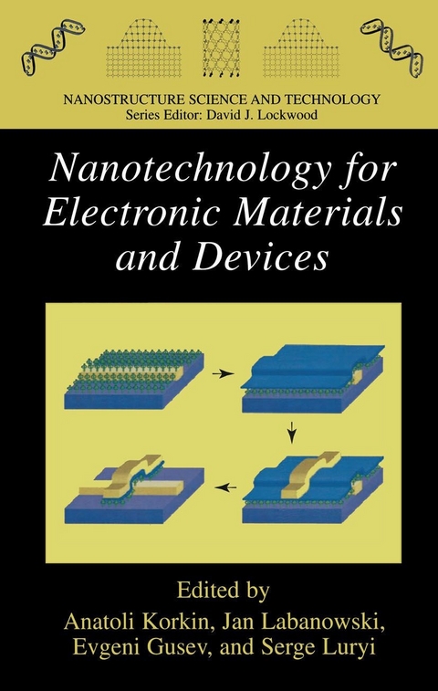
Nanotechnology for Electronic Materials and Devices (eBook)
VIII, 368 Seiten
Springer US (Verlag)
978-0-387-49965-9 (ISBN)
Quickly becoming the hottest topic of the new millennium (2.4 billion dollars funding in US alone)
Current status and future trends of micro and nanoelectronics research
Written by leading experts in the corresponding research areas
Excellent tutorial for graduate students and reference for 'gurus'
Provides a broad overlook and fundamentals of nanoscience and nanotechnology from chemistry to electronic devices
The high level of attention and interest of the global community to NANO science and technology to a large extent is linked to the GIGAntic challenges for the c- tinuing growth of information technology, which sparked an unprecedented level of interdisciplinary and international cooperation among industrial and academic researchers, companies, IT market rivals, and countries, including former political and military rivals . Microelectronics technologies have reached a new stage in their development: The latest miniaturization of electronic devices is approaching atomic dimensions, interconnect bottlenecks are limiting circuit speeds, new ma- rials are being introduced into microelectronics manufacture at an unprecedented rate , and alternative technologies to mainstream complementary metal-oxide sem- conductors (CMOSs) are being considered . The very dynamic stage of science and technology related to the advanced and future electronics and photonics creates a growing gap between the large number of rapid publications and nanotechnology highlights in media on one side and fundamental understanding of underlying phenomena and an adequate evaluation of scientific discoveries and technological innovations on the other side. Writing a tutorial book on fundamentals of science and technology for electronics at this time is almost the same level of challenge as writing a history book during a revolution.
A Hybrid Route from CMOS to Nano and Molecular Electronics.- From SOI Basics to Nano-Size MOSFETs.- Strategies of Nanoscale Semiconductor Lasers.- Silicon Nanocrystal Nonvolatile Memory.- Novel Dielectric Materials for Future Transistor Generations.- Scanning Force Microscopies for Imaging and Characterization of Nanostructured Materials.- Simulation of Nano-CMOS Devices: From Atoms to Architecture.- Lattice Polarons and Switching in Molecular Nanowires and Quantum Dots.
"6 Scanning Force Microscopies for Imaging and Characterization of Nanastructured Materials (p. 223-224)
Bartosz Such, Franci szek Krok, and Marek Szymonski
6.1. INTRODUCTION
The growing tendency to miniaturize devices used in every-day life (e.g., integrated circuits or technologies for optical information transfer), as well as exciting prospects of new emerging technologies (quantum electronics, biochips, etc.) are prompting a huge interest in nanotechnology and the science of nanostructured materials. In particular, there is a need to develop efficient technologies for the preparation of surfaces with desired structure and electronic properties.
In light of those advances, designing analytical and nondestructive tools for the characterization of surface electronic and chemical properties with nanometer resolution is of utmost importance. Such tools are important for both nanostructure characterization and nanomanipulation of small-size assemblies of atoms and/or molecules on crystal surfaces in order to construct nanodevices. Furthermore, local determination of surface morphology and mechanical as well as electronic properties might be important for practical functioning of various nanosensors and nanodevices in biological objects.
6.2. SCANNING PROBE MICROSCOPY
Scanning probe microscopy (SPM) is commonly used for imaging and characterizing surface structure in the range between hundreds of micrometers and a few nanometers with atomic structure details. In some way, it represents the development of the concept of a profilometer. The heart of every SPM is a sharp tip acting as a probe (see Fig. 6.1). The detailed design of its support as well as the interaction that is probed by the tip are dependent on the specific type of SPM. A tip is scanned over a sample (or a sample is scanned against a tip) by a piezoelectric scanner, usually in the form of a tube.
The tube is divided into four sectors along its axis, which bend according to the voltage applied across them. Since the tube is long (up to several centimeters) and typical scan ranges are small (below 100 urn) the curvature of the tip path is negligible. The piezotube is also used for varying the tip-surface distance . Modem designs give an accuracy on the order of picometers in both vertical and horizontal directions. However, for some applications (such as biological studies), scan ranges exceeding 100 urn are required.
For that purpose, SPM designs in which the scanning motion is accomplished by two perpendicular piezoelements are used. In order to control the tip position with an accuracy of picometers, the entire instrument must be rigorously separated from external vibrations. Various systems of spring suspension and eddy current damping are used."
| Erscheint lt. Verlag | 7.5.2010 |
|---|---|
| Reihe/Serie | Nanostructure Science and Technology |
| Zusatzinfo | VIII, 368 p. 232 illus. |
| Verlagsort | New York |
| Sprache | englisch |
| Themenwelt | Naturwissenschaften ► Physik / Astronomie |
| Technik ► Elektrotechnik / Energietechnik | |
| Technik ► Maschinenbau | |
| Schlagworte | CMOS • DRAM • Electronics • Laser • nanostructure • nanotechnology • Non-volatile Memory • quantum dot • Simulation • Transistor |
| ISBN-10 | 0-387-49965-2 / 0387499652 |
| ISBN-13 | 978-0-387-49965-9 / 9780387499659 |
| Haben Sie eine Frage zum Produkt? |
Größe: 21,3 MB
DRM: Digitales Wasserzeichen
Dieses eBook enthält ein digitales Wasserzeichen und ist damit für Sie personalisiert. Bei einer missbräuchlichen Weitergabe des eBooks an Dritte ist eine Rückverfolgung an die Quelle möglich.
Dateiformat: PDF (Portable Document Format)
Mit einem festen Seitenlayout eignet sich die PDF besonders für Fachbücher mit Spalten, Tabellen und Abbildungen. Eine PDF kann auf fast allen Geräten angezeigt werden, ist aber für kleine Displays (Smartphone, eReader) nur eingeschränkt geeignet.
Systemvoraussetzungen:
PC/Mac: Mit einem PC oder Mac können Sie dieses eBook lesen. Sie benötigen dafür einen PDF-Viewer - z.B. den Adobe Reader oder Adobe Digital Editions.
eReader: Dieses eBook kann mit (fast) allen eBook-Readern gelesen werden. Mit dem amazon-Kindle ist es aber nicht kompatibel.
Smartphone/Tablet: Egal ob Apple oder Android, dieses eBook können Sie lesen. Sie benötigen dafür einen PDF-Viewer - z.B. die kostenlose Adobe Digital Editions-App.
Zusätzliches Feature: Online Lesen
Dieses eBook können Sie zusätzlich zum Download auch online im Webbrowser lesen.
Buying eBooks from abroad
For tax law reasons we can sell eBooks just within Germany and Switzerland. Regrettably we cannot fulfill eBook-orders from other countries.
aus dem Bereich
